UV lasers are the best choice for a wide range of PCB applications in a wide range of industrial applications, from the production of the most basic circuit boards, circuit cabling, to the production of pocket embedded chips and other advanced processes are common. The difference in this material makes UV lasers the best choice for a wide range of PCB applications in a wide range of industrial applications, from the production of the most basic circuit boards, circuit wiring, to the production of compact embedded chips and other advanced processes are common.
The UV green laser light works quickly in the production of the circuit, and the surface pattern can be etched on the circuit board in minutes. This makes UV lasers the fastest way to produce PCB samples. The R & D department notes that more and more sample laboratories are equipped with an internal UV laser system. Depending on the optical instrument, the size of the UV laser beam can be 10-20 μm, producing a flexible circuit trace. Although the use of laser beam production circuit is the fastest method of PCB samples, but the large-scale surface etching applications are best left to the chemical process.
Ultraviolet laser cutting is the best choice for large or small production, and it is also a good choice for PCB removal, especially when it is applied to flexible or rigid-flexible circuit boards. Removal is to remove a single circuit board from the panel, taking into account the increasing flexibility of the material, this demolition will face a great challenge. V-slot cutting and automatic circuit board cutting and other mechanical disassembly methods easily damage sensitive and slim substrate, to the electronic professional manufacturing services (EMS) enterprises in the demolition of flexible and rigid and flexible circuit board when the trouble.
UV most powerful laser cutting can not only eliminate the impact of mechanical stress generated during the disassembly process, deformation and damage circuit components, but also less thermal stress than other lasers such as CO2 laser cutting. The reduction of the cutting cushion can save space, which means that the components can be placed closer to the edge of the line, and more lines can be installed on each circuit board to maximize efficiency to the maximum limit of flexible line applications The
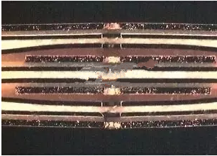
Another application that utilizes UV lasers for small beam size and low stress properties is drilling, including through holes, micropores and blind burrs. The UV laser system drills through the substrate by focusing the vertical beam straight through the substrate. Depending on the material used, holes as small as 10 μm can be drilled. Ultraviolet lasers are particularly useful for multi-layer drilling. Multilayer PCBs are made of hot press using composite materials. These so-called “semi-cured” will be separated, especially after the use of higher temperature green astronomy laser processing.
Another application that demonstrates the versatility of UV lasers is the depth of engraving, which encompasses many forms. With the software control of the laser system, the laser beam is set for controlled ablation, that is, it can be cut on a material at the desired depth, and can be stopped, continued and completed before turning to another depth and starting another task Of the processing. Various in-depth applications include: small-scale production used when embedding the chip and surface removal of the organic material from the metal surface.
UV 500mw green laser is the most striking is the ability to use a single step to complete all of the above applications. What does this mean for making a circuit board? People no longer need to use the same process on different devices and methods to achieve an application, and only a single processing can get complete parts. This streamlined production scheme helps to eliminate the quality control issues that arise when switching between boards in different processes. UV-free debris ablation also means that no post-processing cleaning is required.